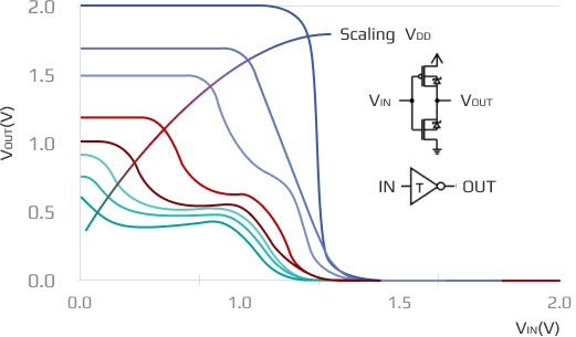
Overview of Ternary Logic
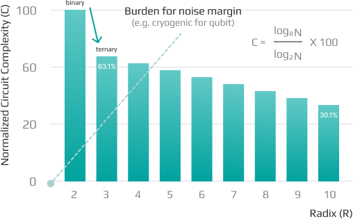
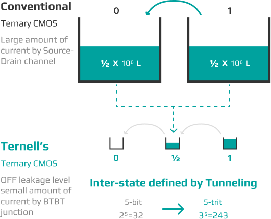
Ternary logic uses trits of {0, 1, 2}, adding one more state to the binary {0, 1} bits, resulting in a 37% reduction in circuit complexity compared to binary. By manufacturing semiconductors based on ternary logic, the number and area of transistors required to build circuits are reduced, which in turn lowers power consumption.
While increasing the radix to 4, 5, etc., can further reduce area and power consumption compared to ternary, there are practical limits due to signal noise and malfunction issues that arise in actual semiconductor fabrication. Although advances in semiconductor technology may change this in the future, with current silicon and transistor-based semiconductor systems, ternary logic is the most cost-effective multi-valued logic system.