로고 로고

Business Area

Business Area

Ternel designs customer success through innovative semiconductor technology and services.

IP Licensing

Business 01 IP Licensing

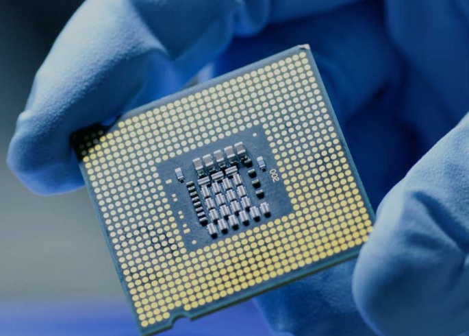
Ternell has transformed its years of research on ternary semiconductor design and manufacturing technologies into intellectual property (IP), which it provides to clients.
Ternell’s proprietary technology enables the fabrication of ternary semiconductors using existing commercial foundry-based CMOS technology. Through effective control of leakage current, this technology allows for reduced chip area, as well as the implementation of low-power, high-efficiency, and high-performance T-CMOS technology.
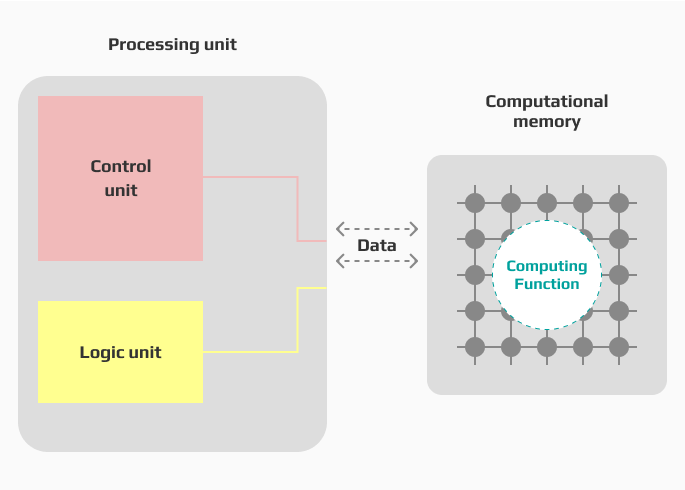
Among ternary semiconductor technologies, Ternell is particularly focused on T-SRAM (Ternary-SRAM), which can be used in various SoCs including AI accelerators. In addition, the company possesses technologies for T-CIM (Ternary-Computing In Memory), T-CAM (Ternary-Content Addressable Memory), and T-PUF (Ternary-Physically Unclonable Function).
Clients can utilize Ternell’s IP through PDKs (Process Design Kits) provided by major domestic and international foundry companies. Ternell, in collaboration with foundry companies and design houses, offers the necessary technical support to its clients.

Design & Engineering

Business 02 Design & Engineering

Ternell possesses specialized process technologies such as ternary semiconductor technology and tunneling current control (off-state tunneling current control), as well as expertise in circuit and system design.
Therefore, in response to clients' advanced AI SoC design requirements, Ternell is able to actively provide design and engineering services based on its proprietary technologies and IP.

PRODUCT LIFECYCLE

Concept

Feasibility

Planning

Execution

Production

Sustaining

EQL

◆ Quality Gates

Silicon Design : By combining conventional semiconductor design techniques with ternary semiconductor design technology, Ternell develops ASIC/layout designs and makes technical decisions across all aspects of the process flow—from high-level design to synthesis, placement and routing, timing, and power consumption.

Design for Manufacturing (DFM) : Ternell applies DFM rules that offer performance advantages based on foundry process characteristics, andutilizes advanced tools and methods to achieve more robust semiconductor designs.

Design for Testability (DFT) : Ternell establishes and applies DFT methodologies across various domains, including digital logic, IP, memory elements, and I/O boundary scanning.

Design for Reliability (DFR) : Ternell continuously develops methodologies to overcome the reduction in degradation robustness and noise margins for products using leading-edge process nodes.

 SoC Design & Production

Business 03 SoC Design & Production

Ternell utilizes a variety of IPs developed through ternary semiconductor technology to build the UniBrainTM Architecture, optimized for AI computing, and designs and manufactures SoCs based on this architecture.

UniBrainTM is designed with a Compute-In-Memory (CIM) approach, where the memory and processing unit themselves are capable of highly efficient computation. This significantly reduces data transfer, resulting in higher performance and much lower power consumption. These characteristics are highly advantageous for AI and high-performance computing workloads.