Why Ternary-SRAM Is Needed
The area Ternell is most focused on, based on its ternary (three-valued) semiconductor technology, is SRAM for on-chip cache memory.
With the recent surge in demand for AI computing, various types of SoC (System on Chip) semiconductors—often referred to as AI accelerators, including GPUs—are being released along with systems that incorporate them.
To develop high-performance AI accelerators, it is important to design high-performance parallel processing circuits such as ALU (Arithmetic Logic Unit) cores, but it is equally crucial to design and utilize an effective memory hierarchy that can support the ALU closely.
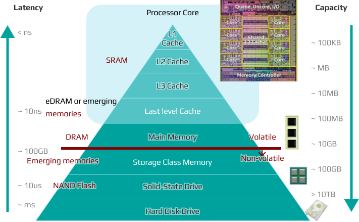
For high-performance SoC semiconductors, the on-chip memory—implemented as cache memory on the same silicon die as the ALU—should be designed with as large a capacity as possible. Although high-performance SRAM is used as on-chip memory, SRAM is bulkier and harder to integrate than DRAM (main memory), and due to heat generation, it is difficult to use in large enough capacities as needed.
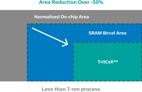
However, by manufacturing on-chip memory using Ternell’s ternary-based SRAM (T-SRAM), both area and power consumption can be reduced by more than 50% at process nodes below 7 nm.
In high-performance SoC semiconductors such as CPUs and GPUs, SRAM used as on-chip cache memory can account for as much as 70–80% of the total chip area. Therefore, such reductions in area and power consumption are highly beneficial for SoC design engineers.
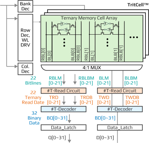
Ternary-SRAM Using Ternary-CMOS
Since firstannouncing successful mass production of Ternary-CMOS in a 110-nm foundry process in 2019 (published in Nature Electronics), Ternell has continued developing its technology and has successfully developed Ternary-SRAM products based on a 28-nm process.
Ternary-SRAM produced using the 28-nm process achieves a read speed of 0.9 ns for L1 cache and 4.2 ns for L2 cache—matching the speed of conventional binary cache SRAM—while reducing area by 33% and power consumption by 51%.
Currently, Ternell has completed the design of products based on the 14-nm process and is testing them, while also jointly developing products below 4 nm with leading global foundry companies.
Binary System Compatibility of Ternary-SRAM
Although Ternary-SRAM is designed based on ternary logic, it can be fabricated on the same silicon die alongside other logic blocks in SoCs designed with binary logic. In other words, Ternary-SRAM can be used as a plug-in module to replace conventional SRAM.
This is possible thanks to Ternell’s fast T-READ/WRITE design IP, which combines a binary-to-ternary T-encoder/decoder. This T-encoder/decoder is a simple combinational logic gate that operates in parallel at the final I/O stage, so it works at high speed regardless of core memory capacity expansion.
As a result, there is almost no delay from binary-to-ternary conversion, and the system operates as if it were composed solely of binary logic. The additional energy required for encoding/decoding is negligible.
Error Correction Methods for Ternary-SRAM
Because the binary-to-ternary converter allows for testing and correction using conventional binary input/output, no additional ternary-specific algorithms or testing setups are required.
- Hard error: Detected by internal BIST (Built-In Self-Test) using march tests, and repaired by hard-wiring redundant columns to dead cell addresses.
- Soft error: Since Ternary-SRAM operates with binary data, conventional binary ECC (Error Correction Code) can be used. An additional bit per word (parity bit) is used for correction based on output results.
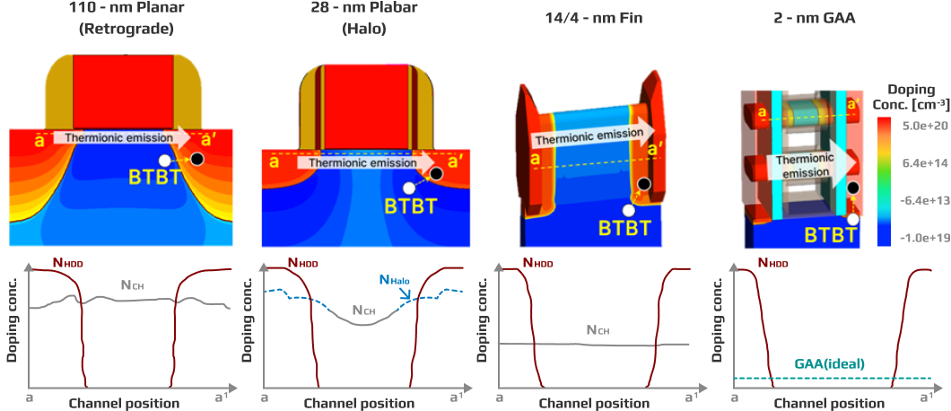
Scaling Down Ternary-SRAM
While conventional binary CMOS faces worsening heat issues as integration increases, SRAM made with Ternell’s ternary technology becomes even more stable as the process node shrinks.
Especially below 14 nm, heat issues in conventional CMOS become severe, but T-CMOS, which operates using tunneling current, can dramatically reduce standby power increases due to heat.
Furthermore, in FinFET structures, the region through which tunneling current flows is separated from the conventional channel, and this separation becomes even clearer in GAA (Gate-All-Around) structures, resulting in more stable operation.
This not only reduces the device’s power consumption but also lessens the ECC burden, which greatly helps improve actual density.